
SPI 101: Serial Peripheral Interface
Introduction
This blog series is focused on SPI hacking with practical application in hardware analysis, firmware extraction, and embedded device inspection. Understanding this protocol is essential before moving on to hands-on tools and extraction techniques, which will be discussed in upcoming parts.
This post is for the curious: the makers, the tinkerers, and the hackers who want to understand what SPI is, how it works, and why it matters in real-world hardware hacking. We’ll cover everything from the basics of the protocol to how it plays into accessing flash memory chips. Whether you’re trying to dump a router’s firmware or dig into an old motherboard.
What is SPI?
SPI stands for Serial Peripheral Interface, a synchronous serial communication protocol used for short-distance communication, primarily in embedded systems. It enables a master device to communicate with one or more slave devices using separate lines for data transmission and clock signaling.
SPI is commonly found in systems involving flash memory, sensors, ADCs, and other digital components. In the context of hardware hacking, it is most frequently used to interface with SPI flash memory chips that store firmware or BIOS data.
Key Features:
- Full-Duplex Communication: Data goes both ways at the same time.
- High Speed: Much faster than protocols like I2C.
- Low Overhead: Just a handful of wires, no need for complex handshakes.
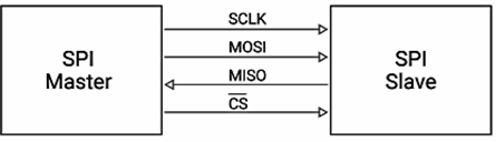
SPI Bus Architecture
The SPI protocol is based on a master-slave architecture. The master initiates communication and controls the clock, while one or more slave devices respond to commands.
Standard SPI Lines
| Signal | Full Name | Direction | Description |
| MOSI | Master Out, Slave In | Master → Slave | Data sent from master to slave |
| MISO | Master In, Slave Out | Slave → Master | Data sent from slave to master |
| SCLK | Serial Clock | Master → Slave | Synchronizes data transmission |
| CS | Chip Select (Active Low) | Master → Slave | Enables specific slave for communication |
Two additional lines, VCC and GND, are required to power the slave device and establish a common ground.
Why SPI is Important in Hardware Hacking
SPI is widely used in flash memory chips found in embedded devices. These memory chips often store the firmware responsible for device operation. Accessing and manipulating this firmware is a critical step in many hardware security assessments.
If you can access that SPI chip physically, you can read or write its contents.
Here are just a few real-world uses:
- Extracting Firmware: Dump the contents for reverse engineering.
- Restoring Bricked Devices: Reflash a corrupt BIOS or bootloader.
- Unlocking Features: Patch firmware to bypass restrictions.
- Security Auditing: Discover hidden functions, credentials, or backdoors.
Typical SPI Flash Chips
Most SPI flash chips follow the 25-series standard (like Winbond W25Q64, Macronix MX25L, etc.) and are often SOIC-8 packages – eight tiny legs soldered onto the board.
You’ll find them on:
- Wi-Fi Routers
- Motherboards (BIOS chips)
- Smart TVs and Set-Top Boxes
- IoT Devices
- Game Consoles
How to Identify an SPI Flash Chip on a PCB
- Look for 8-Pin SOIC Packages:
- Check for Common Markings:
- Manufacturer (e.g., Winbond, Macronix, Atmel)
- Series number (e.g., 25Q64, MX25L8006E, AT25DF321)
- Voltage or capacity (e.g., 3.3V, 8Mbit, 64Mbit)
- Look Near the CPU or Main Controller:
- Use the Chip’s Datasheet:
Most SPI flash chips are in a Small Outline Integrated Circuit (SOIC-8) form factor.
These are small rectangular chips with 8 pins 4 on each side.
Use a magnifying glass or macro camera to read the markings on the chip. Typical identifiers include:
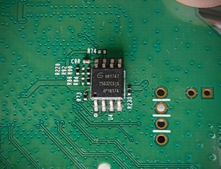
Flash memory is usually placed close to the main processor or system-on-chip (SoC), as it's directly accessed during boot.
Once you identify the part number, search online for its datasheet. This confirms whether it supports SPI and helps you verify the pinout for connection.
SPI Communication Workflow (Simplified and Accurate)
SPI is a step-by-step communication protocol between a master (e.g., CH341A programmer) and a slave (e.g., SPI flash chip). Here's how it works:
- CS (Chip Select) Pulled LOW:
- Command Sent via MOSI:
0x9F– Read chip ID0x03– Read data0x02– Write data- Clock Signals via SCLK:
- Chip Responds via MISO:
- CS Pulled HIGH:
Activates the target chip. Only the chip with CS pulled low will respond.
The master sends an instruction (e.g., Read, Write, Erase) over the MOSI line.
Example commands:
The master sends clock pulses over the SCLK line.
Each bit of data sent or received is synchronized with one clock pulse.
The slave sends data back over MISO (e.g., firmware data, chip ID).
Ends the communication. The chip stops responding and resets its SPI interface.
Summary of SPI Lines:
- CS: Selects the chip (active LOW)
- MOSI: Master sends data/commands to the chip
- MISO: Chip sends data back to the master
- SCLK: Clock signal for data synchronization
This process repeats during firmware reading or writing, handled automatically by software tools like Flashrom.
Risks and Considerations
When working with SPI flash chips, always follow proper electrical and handling precautions:
- Voltage Compatibility: Use the correct voltage (3.3V or 1.8V).
- Avoid Dual Powering: Never power from two sources.
- Pin Orientation: Ensure correct alignment of pin 1 when connecting clips or probes.
- Data Integrity: Perform multiple reads and compare results to verify accuracy.
Applying SPI Knowledge in Real-World Hacking
Understanding how SPI works is essential before attempting to read or write firmware. In real hardware hacking scenarios, this knowledge helps you:
- Correctly identify and connect to flash memory chips.
- Know what each pin does, preventing wiring mistakes.
- Understand what’s happening when tools like Flashrom send commands.
- Troubleshoot issues like failed reads, bad connections, or mismatched voltages.
In practice, this means you'll be able to confidently interact with SPI flash chips, extract firmware binaries, and analyze them which is the core of many hardware security tasks.
Conclusion
This post introduced the core concepts of SPI communication and how it's used in hardware hacking. We explored how SPI works, how to identify flash chips, and key considerations when handling them. Understanding these fundamentals is essential before attempting to interface with real hardware.
In the next post, we’ll move from theory to practice. You’ll learn about the tools needed to work with SPI flash memory, how to identify the correct chip, make proper physical connections, use appropriate software, and ultimately extract the firmware (bin) file from a device.

Address:
601, park plaza business center, S No. 296/2, Porwal Rd, Lohegaon, Pune, Maharashtra 411047
Phone: 91 9152445255
Email: [email protected]
GET IN TOUCH:
©Copyright 2024 Unoacademy Labs LLP